TL;DR
Thorsten Meyer AI published a 3D explainer on Nov. 22, 2026, showing how AI accelerators combine compute dies, stacked high-bandwidth memory, an interposer, a substrate and cooling. Vendor specifications cited in the article point to growing memory bandwidth and complex packaging; the piece says memory and packaging capacity can constrain supply, while some future product details and production limits remain unsettled.
Thorsten Meyer AI published a 3D explainer on Nov. 22 showing how an AI accelerator can combine multiple compute dies, stacked high-bandwidth memory, a silicon interposer, a package substrate and cooling hardware. Drawing on vendor documents, the report argues that memory bandwidth and advanced packaging, as well as compute capacity, help determine how quickly AI systems can run and how many accelerators suppliers can deliver.

Get business pricing on tech for your team
- Business-only prices and quantity discounts
- Tax-exempt purchasing
- Multiple users, one account, clear invoices
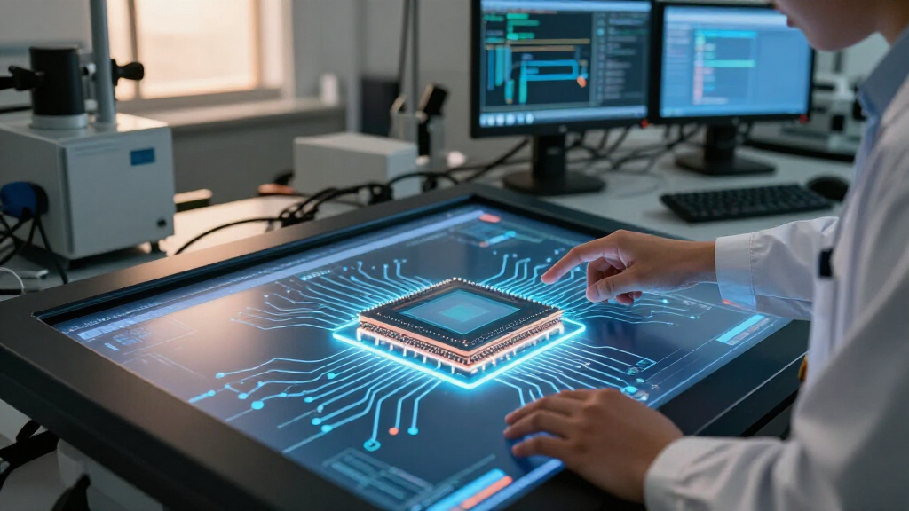
The explainer uses a 3D model to present an accelerator package layer by layer. It depicts a substrate at the base, a silicon interposer above it, compute dies and high-bandwidth memory (HBM) stacks, and a cold plate for liquid cooling. The publisher says the layer order and component counts follow vendor documentation, while all dimensions are schematic: the cited manufacturers do not publish the relevant package and die measurements in millimetres, so the model does not assign them.
Vendor designs differ. The article says Nvidia’s Rubin GPU uses two reticle-limited compute dies and cites Nvidia’s architecture blog for a total of 336 billion transistors. It describes AMD’s MI350 Series as using eight vertically stacked accelerator complex dies and two I/O dies; the MI355X is listed at 185 billion transistors. AMD’s CDNA 4 white paper is also cited for eight HBM stacks on the MI355X. These figures describe specific products and vendor materials, not a universal AI-chip layout.
HBM consists of DRAM dies stacked above a base die and linked vertically by through-silicon vias, or TSVs. The interposer provides dense connections between memory and compute dies. The report cites TSMC’s description of CoWoS-S packaging, including an interposer area of up to about 2,700 square millimetres, and describes CoWoS-L as a way to connect silicon bridges in a carrier layer. It also cites Nvidia’s product page for a rise in stated memory bandwidth from 900 GB/s for V100 to 19.2 TB/s for Rubin. Those are vendor specifications for different generations, not an independent performance comparison.

Memory and Packaging Set the Pace
The explainer’s central point is that processor speed alone does not describe an AI accelerator’s capabilities. Compute dies need data, and HBM bandwidth helps feed them. The physical links between memory and compute, along with the package that holds them together, are part of the system’s design and manufacturing challenge.
Packaging also has industrial consequences. The report describes large silicon interposers and more complex chip stacking, and cites TSMC’s statements about producing packages larger than a single reticle area. These processes require specialized manufacturing capacity. If that capacity is constrained, it can limit the supply of complete accelerators even when demand for AI computing remains strong.
The article quotes SK hynix as expecting demand for memory to exceed supply “through 2030.” That is a company outlook, not a confirmed forecast of how much memory will be available or what prices buyers will pay. For businesses planning AI infrastructure, the report suggests that memory and packaging availability deserve attention alongside processor specifications. It does not provide purchase prices, delivery schedules or a quantified estimate of their effect on system costs.
Products Worth Considering

Bose QuietComfort Ultra Headphones Gen 1, Lunar Blue

Apple MacBook Air 13-inch Laptop with M5 Chip, 16GB Memory, 512GB SSD, Liquid Retina Display, and 12MP Center Stage Camera (Midnight)

Apple Watch Series 12 GPS 42mm Smartwatch
As an affiliate, we earn on qualifying purchases.
From Silicon Dies to Full Racks
A silicon die is the individual piece of semiconductor containing circuits. A reticle is the maximum area a lithography scanner can expose in one step; manufacturers can combine dies or use packaging techniques to build larger systems. The article says Blackwell Ultra uses two reticle-sized dies connected by a die-to-die link, and cites Nvidia for 208 billion transistors. Its discussion of Rubin concerns a later product generation and cites Nvidia for two compute dies and 336 billion transistors.
HBM stacks put memory close to compute. TSVs carry signals vertically through the stacked DRAM, while the interposer connects components across the package. JEDEC’s HBM4 standard, published in April 2025 according to the source, permits stacks of four, eight, 12 or 16 layers and up to 64 GB per stack. Those standard limits do not mean every product uses the maximum stack height or capacity.
The report also zooms out from a package to a rack. It cites NVIDIA’s DGX GB user guide and AMD’s CDNA 4 white paper for system counts, and says eight AMD accelerator modules sit on a universal baseboard connected through Infinity Fabric. The model’s rack outline comes from an Open Compute Project listing. Those system illustrations are schematic, and the hardware counts cited for different vendors should not be read as a direct comparison of equivalent systems.
““large silicon interposer area to accommodate various functional top dies, including logic chiplets, with high-bandwidth memory (HBM) cubes stacked over it””
— TSMC, describing CoWoS-S
Limits of the Model and Forecasts
The 3D model does not provide real-world dimensions for dies, packages or memory stacks. The publisher says manufacturers do not disclose those measurements in the sources used, so the model’s sizes are schematic. It illustrates component relationships rather than manufacturing tolerances or the exact appearance of a commercial package.
Some forward-looking claims are also not independently verified in the article. It reports that TSMC’s chief executive said on Oct. 15, 2026, that the company was in “real world production of 5x reticle size” and working on 9x and 14x. The article does not include details on production volume, customer allocation or when those larger formats may be available. AMD’s statements about MI455X and MI450X packaging likewise describe future products; their final configurations and availability are not established here.
The cited bandwidth figures come from Nvidia product information, and the supply outlook comes from SK hynix. The report does not independently measure performance, quantify the scale of any shortage or establish how packaging capacity will affect prices and delivery times. Its source material’s cooling description says the MI355X platform is supplied with a cold plate, but the supplied text cuts off before giving the full detail.
Next Steps for Chip Production
The next developments to watch are the commercial rollout of newer accelerator generations, the production capacity available for advanced packaging, and whether HBM supply meets demand. The source does not give launch dates or delivery milestones for the cited future AMD products, nor does it specify when TSMC’s larger interposer formats will reach broader production.
For readers evaluating AI systems, product specifications and supplier updates will clarify the memory capacity, bandwidth, package design and cooling requirements of each configuration. The claims in this explainer can be revisited as manufacturers publish fuller documentation and systems reach customers. Current evidence supports the layer-by-layer description; the scale and duration of any supply constraints remain uncertain.
Key Questions
What does an AI accelerator package contain?
In the designs described here, it can contain compute dies, HBM stacks, a silicon interposer and a package substrate, with cooling hardware above. The exact arrangement varies by product.
What is HBM?
High-bandwidth memory is DRAM arranged in vertical stacks and connected with through-silicon vias. Placing the stacks close to compute dies gives the package a high-bandwidth memory connection.
What does the interposer do?
The interposer is a thin silicon wiring layer that links compute dies and memory. The report describes TSMC’s CoWoS packaging as one approach to building these connections across large packages.
Are the 3D model’s chip dimensions exact?
No. The publisher says the dimensions are schematic because the cited vendor materials do not provide measurements for the dies, package or memory stacks.
Is an AI chip shortage confirmed through 2030?
The article cites SK hynix’s expectation that memory demand will exceed supply through 2030. That is a company outlook; the report does not independently confirm the forecast or quantify its effects.
Source: Thorsten Meyer AI